Hierarchy of the DRAM Subsystem

Every channel has its own memory controller that means it has its own address, command, and data bus.

In a rank, the address and command bus are shared to all chips, but the data bus is dedicated to a chip. Therefore the rank can offer a wide interface.

In a chip, all of the address, command, and data bus are shared to banks. However, in each bank, the address, command, and data are latched, and each bank operates its own command.

A column can be accessed when a row is open(activated).


DRAM Operation

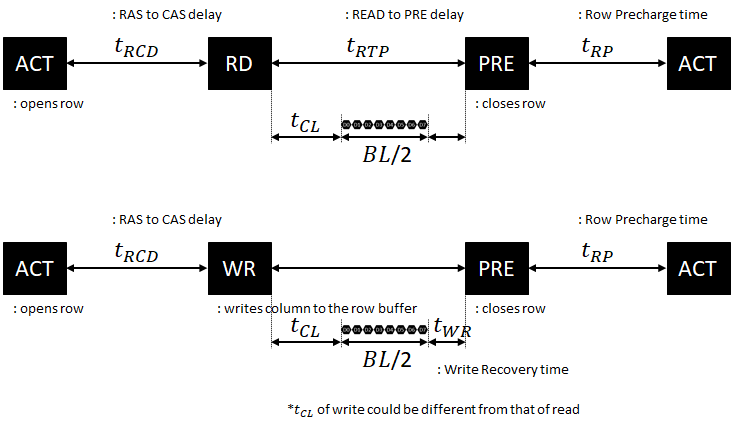
DRAM Operation starts with row activation. Activating a row means select and open a row of DRAM cells in a specific bank and then the data could be accessed through row buffer(which is also called sense amplifier) in size of a column. When accessing a row is finished then, the row should be precharged(closed) for activating another row. 

The most critical timing parameters of DRAM are tRCD, tCL, tRP. tRCD stands for RAS to CAS delay time which means activating a row is finished and the row is ready to read or write, after tRCD from the ACT(Activation) command. Once RD(Read) or WR(Write) command, data could be transferred after tCL. And when accessing a row is finished, the PRE(Precharge) command should be followed. Precharging a row takes tRP. 

Because the row address is transferred with ACT command and the column address is transferred with RD/WR, which means that row and column address are not used simultaneously, address pins could be shared. 


DRAM Bank Structure

DRAM Bank is a set of rows and columns, which operates a command. A DRAM chip consists of multiple banks, and each bank could operate its own command. However, the command, address, data pins are shared to all of the banks, and all of DRAM commands are synchronized, DRAM operations could be pipelined. With pipelining, bank structure is good for hiding long latency of DRAM(tRCD, tCL, tRP, etc).

This is a logical structure of a DRAM Bank. All of the pin counts are referenced from Micron DDR4 8Gb X8 DRAM Chip. In this case, a DRAM bank consists of 64K rows and 1K columns. This chip has 8 bit of data pin, generally, 8 of chips are combined into a DIMM. With 8 chips, each of 8 data pins, and 8 burst length, 64Byte of data could be read or write at single DRAM command. Row buffer size is 8Kb for each chip. 

This is a functional block diagram from Micron DDR4 8Gb X8 DRAM chip. Note that it is a chip. Because DDR4 uses 8 burst length, it seems that 64 bit of data in the row buffer could be transferred to FIFO, in a operation. The LSB 3 bits of column address are discarded, and 8 columns, each of 8 bits are accessed at once.

'Programming > Computer Architecture' 카테고리의 다른 글

Cache write policies  (0) 2022.10.31

일반적인 Linux 배포판을 쓰지 않고, Kernel source와 Root file system 으로 부터 Linux system 을 구성한 경우,

Linux runtime 에 kernel module을 compile 하여 insmod/rmmod 를 할 수 있다.


Kernel module을 컴파일 하기 위해서는 현재 Linux system 에서 사용되고 있는 kernel source를 필요로 한다.

일반적인 방법과 유사하게 사용하기 위해

kernel source 를 /usr/src 디렉토리에 위치시키고,

/lib/modules/<kernel_version>/build 와 symbolic link 시킨다.

# cd /lib/modules/<kernel_version>

# ln -s /usr/src/<kernel_source_dir> build

커널 모듈을 컴파일 하기 위한 준비 작업은 아래 와 같다.

# cd /usr/src/<kernel_source_dir>

# make <defconfig>

# make prepare

# make scripts

※ 참조: http://www.fun25.co.kr/blog/linux-ubuntu-14-04-kernel-module-compile


kernel module을 컴파일 할 Makefile은 아래와 같이 구성한다.

obj-m := test_module.o


all:

make -C /lib/modules/<kernel_version>/build M=$(PWD) modules

clean:

make -C /lib/modules/<kernel_version>/build M=$(PWD) clean

아래는 테스트를 위한 기본적인 kernel module source code.

#include <linux/module.h>

#include <linux/kernel.h>


int init_module(void){

printk(KERN_ALERT"Hello"\n);

return 0;

}


void cleanup_module(void){

printk(KERN_ALERT"Bye"\n);

}


kernel module을 컴파일 하고, insmod/rmmod 를 통해 test 한다.

# make

# insmod <kernel_module>.ko

# rmmod <kernel_module>.ko

※ 이 때, 현재 Linux system 에서 사용되는 kernel 과 다른 source로 부터 kernel module을 컴파일 하게 되면 version 차이로 오류가 나타난다.

'Programming > Linux Kernel' 카테고리의 다른 글

cross kernel debugging  (0) 2020.06.19
Kernel module programming  (0) 2018.05.23
Kernel Version Check  (0) 2018.05.23
Kernel 프로그래밍 - printk  (0) 2017.06.20

Ubuntu 에서 Headless browser 인 PhantomJS를 설치하는 방법을 소개한다.


PhantomJS는 기본적으로 Multi platform 을 지원하여, Windows, Linux, FreeBSD 등 다양한 OS 상에서 구동 될 수 있다.

Architecture / OS 에 따라 기본적으로 제공되는 파일을 사용하여 설치 할 수 없는 경우

Github 로 부터 source code를 다운 받아 설치 할 수 있다.


PhantomJS에서 필요한 패키지(Qt, WebKit 등)를 자동으로 설치 하기 떄문에 Dependency가 없다고 하지만,

Ruby, gperf 등 일부 패키지를 설치 하지 않으면 install 도중 Error를 맞이하게 된다.


Prerequisites

1. Ruby Installation

Ruby install은 RVM(Ruby Version Manager)를 통해 할 수 있다. 따라서, Ruby install 을 위한 RVM install 이 필요하다. 

gpg --keyserver hkp://keys.gnupg.net --recv-keys 409B6B1796C275462A1703113804BB82D39DC0E3

$ cd /tmp && \curl -sSL https://get.rvm.io -o rvm.sh

$ cat /tmp/rvm.sh | bash -s stable

*참조: https://www.rosehosting.com/blog/install-ruby-on-rails-on-ubuntu-16-04/

RVM이 설치 되면, Ruby를 설치 할 수 있다. 


RVM 실행

$ source /usr/local/rvm/scripts/rvm


RVM에서 설치 가능한 Ruby version 확인

$ rvm list known


Ruby 설치(stable 최신 버전 2.5.1, 2018.12.10 기준)

$ rvm install 2.5.1


2. Gperf Installation

$ sudo apt-get install gperf


Git source Fetch

$ git clone https://github.com/ariya/phantomjs


PhantomJS Installation from source

$ cd phantomjs

$ ./build.py 

(시간이 꽤 걸린다.)

'Programming > Linux' 카테고리의 다른 글

Piping ls to cp  (0) 2020.12.02
How to use GDB  (0) 2020.03.12
Linux screen  (0) 2018.09.27
Xshell + Xming  (0) 2018.09.10
Memtester  (0) 2018.07.15

+ Recent posts